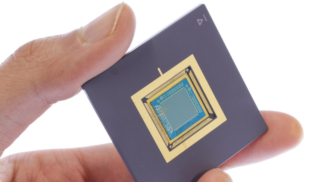
Redefining energy efficiency in data processing

© 2023 EPFL
Developed by EPFL researchers, the first large-scale in-memory processor using 2D semiconductor materials could substantially cut the ICT sector’s energy footprint.
As information and communication technologies (ICT) process data, they convert electricity into heat. Already today, the global ICT ecosystem’s CO2 footprint rivals that of aviation. It turns out, however, that a big part of the energy consumed by computer processors doesn’t go into performing calculations. Instead, the bulk of the energy used to process data is spent shuttling bytes between the memory to the processor.
In a paper published in the journal Nature Electronics, researchers from EPFL’s School of Engineering in the Laboratory of Nanoscale Electronics and Structures (LANES) present a new processor that tackles this inefficiency by integrating data processing and storage onto a single device, a so-called in-memory processor. They broke new ground by creating the first in-memory processor based on a two-dimensional semiconductor material to comprise more than 1000 transistors, a key milestone on the path to industrial production.
Von Neuman’s legacy
According to Andras Kis, who led the study, the main culprit behind the inefficiency of today’s CPUs is the universally adopted von Neumann architecture. Specifically, the physical separation of the components used to perform calculations and to store data. Because of this separation, processors need to retrieve data from the memory to perform calculations, which involves moving electrical charges, charging and discharging capacitors, and transmitting currents along lines – all of which dissipate energy.
Until around 20 years ago, this architecture made sense, as different types of devices were required for data storage and processing. But the von Neumann architecture is increasingly being challenged by more efficient alternatives. “Today, there are ongoing efforts to merge storage and processing into a more universal in-memory processors that contain elements which work both as a memory and as a transistor,” Kis explains. His lab has been exploring ways to achieve this goal using molybdenum disulfide (MoS2), a semiconductor material.
A new two-dimensional processor architecture
In their Nature Electronics paper, Guilherme Migliato Marega, doctoral assistant at LANES, and his co-authors present an MoS2-based in-memory processor dedicated to one of the fundamental operations in data processing: vector-matrix multiplication. This operation is ubiquitous in digital signal processing and the implementation of artificial intelligence models. Improvements in its efficiency could yield substantial energy savings throughout the entire ICT sector.
Their processor combines 1024 elements onto a one-by-one-centimeter chip. Each element comprises a 2D MoS2transistor as well as a floating gate, used to store a charge in its memory that controls the conductivity of each transistor. Coupling processing and memory in this way fundamentally changes how the processor carries out the calculation. “By setting the conductivity of each transistor, we can perform analog vector-matrix multiplication in a single step by applying voltages to our processor and measuring the output,” explains Kis.
A big step closer to practical applications
The choice of material – MoS2 – played a vital role in the development of their in-memory processor. For one, MoS2 is a semiconductor – a requirement for the development of transistors. Unlike silicon, the most widely used semiconductor in today’s computer processors, MoS2 forms a stable monolayer, just three atoms thick, that only interacts weakly with its surroundings. Its thinness offers the potential to produce extremely compact devices. Finally, it’s a material that Kis’s lab knows well. In 2010, they created their first single MoS2 transistor using a monolayer of the material peeled off a crystal using Scotch tape.
Over the past 13 years, their processes have matured substantially, with Migliato Marega’s contributions playing a key role. “The key advance in going from a single transistor to over 1000 was the quality of the material that we can deposit. After a lot of process optimization, we can now produce entire wafers covered with a homogenous layer of uniform MoS2. This lets us adopt industry standard tools to design integrated circuits on a computer and translate these designs into physical circuits, opening the door to mass production,” says Kis.
Revitalizing European chip manufacturing
Aside from its purely scientific value, Kis sees this result as a testament to the importance of close scientific collaboration between Switzerland and the EU, in particular in the context of the European Chips Act, which aims to bolster Europe’s competitiveness and resilience in semiconductor technologies and applications. “EU funding was crucial for both this project and those that preceded it, including the one that financed the work on the first MoS2 transistor, showing just how important it is for Switzerland,” says Kis.
“At the same time, it shows how work carried out in Switzerland can benefit the EU as it seeks to reinvigorate electronics fabrication. Rather than running the same race as everyone else, the EU could, for example, focus on developing non-von Neumann processing architectures for AI accelerators and other emerging applications. By defining its own race, the continent could get a head start to secure a strong position in the future,” he concludes.
Marega, G. M., Ji, H. G., Wang, Z., Pasquale, G., Tripathi, M., Radenovic, A., & Kis, A. (2023). Large-Scale Integrated Vector-Matrix Multiplication Processor Based on Monolayer MoS2. Nature Electronics. DOI: http://dx.doi.org/10.1038/s41928-023-01064-1