Paper alert - Boosting the performance and lifetime of tandems !

© 2024 AM
PV-Lab is happy to share that our latest paper "A Universal Perovskite/C60 Interface Modification via Atomic Layer Deposited Aluminum Oxide for Perovskite Solar Cells and Perovskite–Silicon Tandems" has been published in Advanced Materials !
PV-Lab is happy to share that our latest paper "A Universal Perovskite/C60 Interface Modification via Atomic Layer Deposited Aluminum Oxide for Perovskite Solar Cells and Perovskite–Silicon Tandems" has been published in Advanced Materials !
A big thanks to all the co-authors Kerem Artuk*, Deniz Turkay, Mounir D. Mensi, Julian A. Steele, Daniel A. Jacobs, Mostafa Othman, Xin Yu Chin, Soo-Jin Moon, Ayodhya N. Tiwari, Aïcha Hessler-Wyser, Quentin Jeangros, Christophe Ballif, and Christian M. Wolff* for the fruitful collaboration!
Highlights from the article;
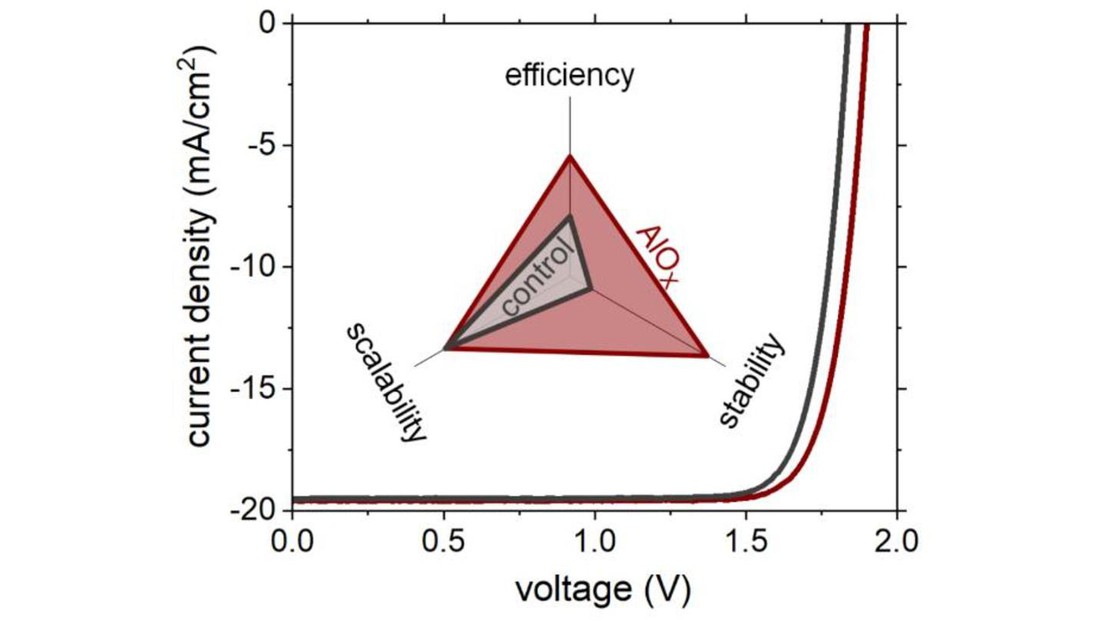
'The primary performance limitation in inverted perovskite-based solar cells is the interface between the fullerene-based electron transport layers and the perovskite. Atomic layer deposited thin aluminum oxide (AlOX) interlayers that reduce nonradiative recombination at the perovskite/C60 interface are developed, resulting in >60 millivolts improvement in open-circuit voltage and 1% absolute improvement in power conversion efficiency. Surface-sensitive characterizations indicate the presence of a thin, conformally deposited AlOx layer, functioning as a passivating contact. These interlayers work universally using different lead-halide–based absorbers with different compositions where the 1.55 electron volts bandgap single junction devices reach >23% power conversion efficiency. A reduction of metallic Pb0 is found and the compact layer prevents in- and egress of volatile species, synergistically improving the stability. AlOX-modified wide-bandgap perovskite absorbers as a top cell in a monolithic perovskite–silicon tandem enable a certified power conversion efficiency of 29.9% and open-circuit voltages above 1.92 volts for 1.17 square centimeters device area.'
Open-access link to the paper: Link