Organic Semiconductor Thin Films and Transistors

© 2017 EPFL
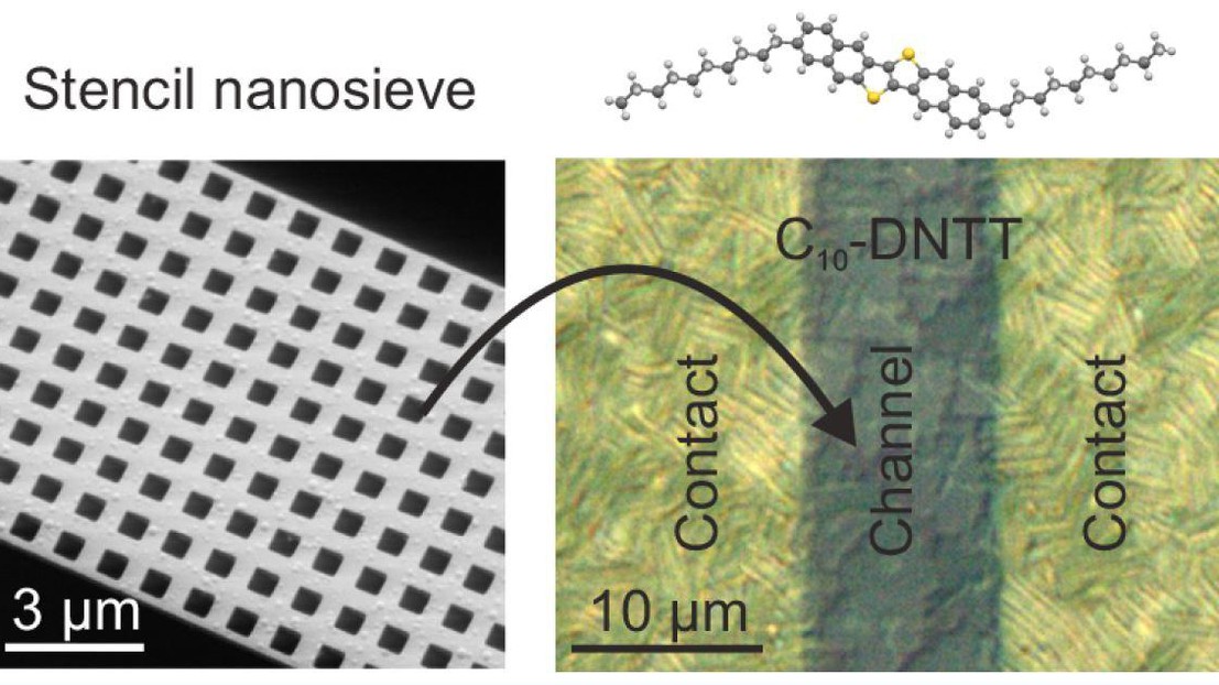
Congratulations to Valentin Flauraud and co-authors for their publication in ACS Appl. Mater. Interfaces entitled "Growth Of Organic Semiconductor Thin Films with Multi-Micron Domain Size and Fabrication of Organic Transistors Using a Stencil Nanosieve".
To grow small molecule semiconductor thin films with domain size larger than modern-day device sizes, we evaporate the material through a dense array of small apertures, called a stencil nanosieve. The aperture size of 0.5 μm results in low nucleation density, whereas the aperture-to-aperture distance of 0.5 μm provides sufficient crosstalk between neighboring apertures through the diffusion of adsorbed molecules. By integrating the nanosieve in the channel area of a thin-film transistor mask, we show a route for patterning both the organic semiconductor and the metal contacts of thin-film transistors using one mask only and without mask realignment.