New technique improves artificial photosynthesis

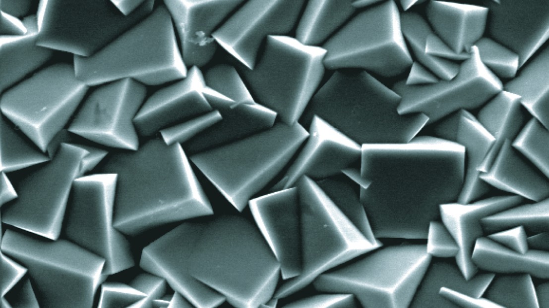
Cuprous oxyde © 2011 EPFL/LPI
Transforming solar energy into a usable form is a real challenge. One technique is to use semiconductors to store the energy as hydrogen. Unfortunately, the most efficient semiconductors are not the most stable. An EPFL team has just discovered that it is possible to protect the semiconductor with a uniform layer just a few nanometers thick.
This discovery will make it possible to improve photoelectrochemical cells. In the same way that plants use photosynthesis to transform sunlight into energy, these cells use sunlight to drive chemical reactions that ultimately produce hydrogen from water. The process involves using a light-sensitive semi-conducting material such as cuprous oxide to provide the current needed to fuel the reaction. Although it is not expensive, the oxide is unstable if exposed to light in water. Research byAdriana Paracchino and Elijah Thimsen, published May 8, 2011 in the journal Nature Materials, demonstrates that this problem can be overcome by covering the semiconductor with a thin film of atoms using the atomic layer deposition (ALD) technique.
Under the supervision of Professor Michael Grätzel in EPFL’s Laboratory of Photonics and Interfaces, the two scientists achieved this remarkable feat by combining techniques used at the industrial scale, and then applying them to the problem of producing hydrogen. With their process, cuprous oxide can be simply and effectively protected from contact with water, making it possible to use it as a semiconductor. The advantages are numerous: cuprous oxide is abundantly available and inexpensive; the protective layer is completely impermeable, regardless of the roughness of the surface; and the process can easily be scaled up for industrial fabrication.
A promising technique
The research team developed the technique by “growing” layers of zinc oxide and titanium oxide, one atom-thick layer at a time, on the cuprous oxide surface. By using the ALD technique, they were able to control the thickness of the protective layer down to the precision of a single atom over the entire surface. This level of precision guarantees the stability of the semiconductor while preserving all of its hydrogen-producing efficiency. The next step in the research will be to improve the electrical properties of the protective layer.
Using widely available materials and techniques that can be easily scaled up brings the “green” photoelectrochemical production of hydrogen closer to the industrial interest.
Source:
Highly active oxide photocathode for photoelectrochemical water reduction, Adriana Paracchino, Vincent Laporte, Kevin Sivula, Michael Grätzel and Elijah Thimsen, Nature Materials, 8 mai 2011.
DOI: 10.1038/NMAT3017
Links:
http://www.nature.com/nmat/journal/vaop/ncurrent/full/nmat3017.html
http://lpi.epfl.ch/


