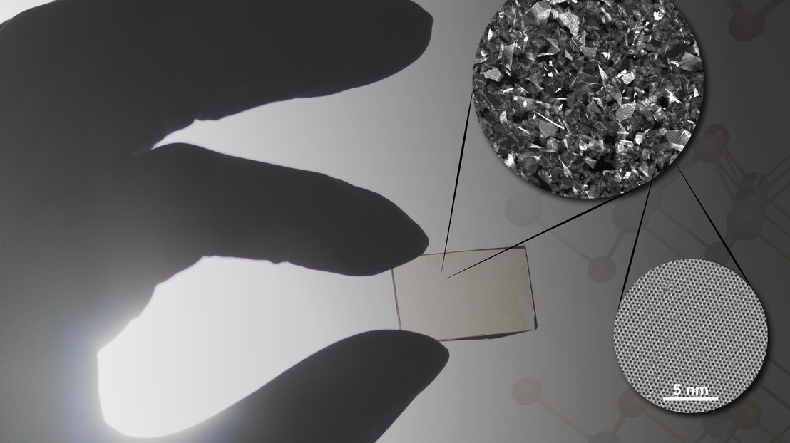
LIMNO develops a route for making 2D nanosheets with fewer defects

© LIMNO 2022 EPFL
Semiconducting 2D transition metal dichalogenide (2D-TMD) nanosheets are promising materials for ultrathin optoelectronic devices, but most scalable routes lead to defective nanosheets and disappointing performance. Now, in a new article, Rebekah Wells of the LIMNO lab and her colleagues have presented a new solution processable method which uses an electrochemical pellet intercalation (ECPI) technique to make high quality nanosheets with fewer defects and higher quantum efficiencies.
The exceptional properties of semiconducting nanosheets of transition metal dichalcogenides (TMDs) make them promising for next generation optoelectronic applications. In order to maintain these properties, it is important to carefully prepare nanosheets with as few defects as possible. Solution processable routes offer a scalable route, but often require harsh processing conditions which damage the nanosheets and hinder their optoelectronic performance. To this effect members of LIMNO developed a solution processable route which produces large-area, thin TMD nanosheets with fewer defects. The method, short-named ECPI, involves taking commercially available powder, pressing it into a compact pellet, and applying an electrical bias to intercalate large molecule cations in between the layered sheets of the TMD. Subsequent gentle agitation produces the nanosheets which can then be processed into thin films for optoelectronic devices. In the case of TMD MoS2 researchers used this method to make field-effect transistors with high charge mobilities (0.2 cm2 V-1 s-1) and photoelectrodes with high internal photon-to-chemical conversion rates (up to 90%). In collaboration with members of CIME and LBEN at EPFL, research showed that these ECPI-made nanoflakes possess at least three times fewer defects than traditional solution processable routes (sonication). As this method can be easily adapted for a range of TMD materials it paves the way towards large-area, high-performing optoelectronic devices. The work has been published in the journal ACS Nano.