Large-Area Solar Energy Conversion with Semiconducting 2D TMDs

© K. Sivula / EPFL 2016
Yu and Sivula publish perspective in new journal: ACS Energy Letters
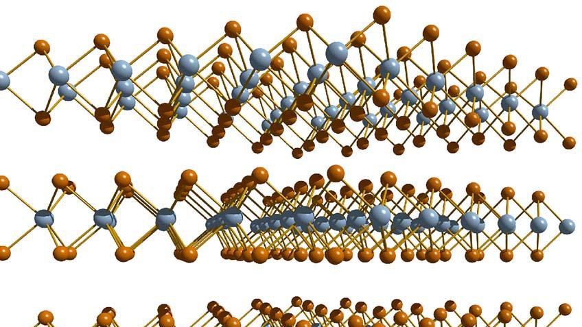
The recently discovered unique optoelectronic properties and chemical robustness of mono- or few-layer two-dimensional (2D) semiconducting transition metal dichalcogenides (TMDs) such as MoS2, WS2, MoSe2, and WSe2 have opened new possibilities for solar energy conversion devices. However, solar energy conversion on a globally relevant scale with TMDs requires the ability to fabricate high-performance large-area thin films of these materials using scalable, low-cost techniques, which remains an ongoing challenge. In this Perspective, the classic properties as well as the new opportunities afforded by the 2D nature of TMDs for photovoltaic and photoelectrochemical applications are presented. State-of-the-art methods for preparing TMD thin films and devices over large areas are compared and scrutinized. The need for increased fundamental understanding of defect states, grain boundaries, interfacial effects, photogenerated charge carrier dynamics, and improved control over thin film morphology/quality are identified as challenges remaining to be addressed, and routes to enabling global-scale solar energy conversion with these materials are suggested. Click here to read the full text!