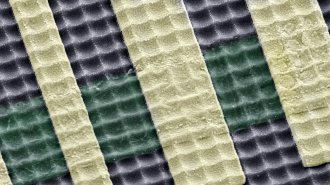
Grayscale nanotopography for improved performance in 2D transistors

© Microsystems Lab EPFL
A team of researchers led by Jürgen Brugger, head of the Microsystems Laboratory in the School of Engineering, has published a new paper that describes a novel approach to improving the performance of next-generation transistors made from two-dimensional semiconducting materials.
Until now, 2D transistors have been seriously limited by electron-phonon scattering; a phenomenon that reduces electron mobility. In a new study from the Microsystems Laboratory, Jürgen Brugger and his team tackled this problem by introducing tensile strain into 2D materials with thermal scanning probe lithography, which they used to create grayscale nanopatterns in a layer of dielectric material. The tensile strain induced by this nanostructure reduced electron-phonon scattering, achieving an 8-fold increase in mobility compared to an unstrained nanostructure.
The researchers see applications for this advancement in the nanofabrication of next-generation nanoelectronic and optoelectronic devices. The findings have been published Nature Communications.
This work builds on a paper published earlier this year in Microsystems & Nanoengineering, which reported an innovative grayscale nanolithography technique combining nanowriting in thermal resist and plasma dry etching with substrate cooling. The method achieved up to 10-fold amplification of polymer nanopatterns into silicon dioxide without proportionally increasing surface roughness, highlighting its potential for applications in photonic and nanoelectronic device fabrication.
Liu, X., Erbas, B., Conde-Rubio, A. et al. Deterministic grayscale nanotopography to engineer mobilities in strained MoS2 FETs. Nat Commun 15, 6934 (2024). https://doi.org/10.1038/s41467-024-51165-4
Erbas, B., Conde-Rubio, A., Liu, X. et al. Combining thermal scanning probe lithography and dry etching for grayscale nanopattern amplification. Microsyst Nanoeng 10, 28 (2024). https://doi.org/10.1038/s41378-024-00655-y