First fully vertical gallium nitride transistors on silicon

© E. Matioli / 2019 EPFL
Our work on the first demonstration of fully vertical gallium nitride transistors on silicon was featured in Semiconductor Today magazine
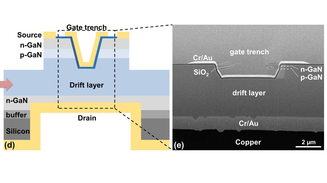
Switzerland’s École Polytechnique Fédérale de Lausanne (EPFL) has claimed the first demonstration of fully vertical gallium nitride (GaN) metal-oxide-semiconductor field-effect transistors (MOSFETs) on silicon (Si) [Riyaz Abdul Khadar et al, IEEE Electron Device Letters, online publication 22 January 2019].
Vertical devices are desired to take advantage of the large critical electric field, high electron mobility and saturation velocity, and high-temperature capability of GaN. Compared with lateral devices, vertical structures are more compact and the peak electric field tends to occur inside the bulk of the semiconductor rather than at surfaces. Unfortunately, the vertical format has generally used prohibitively expensive bulk or free-standing GaN substrates to avoid leakage paths through threading dislocations. Use of silicon significantly reduces material costs, while the larger-diameter substrates should also lead to processing savings in mass production.
Here ,fully-vertical GaN-on-Si MOSFETs were demonstrated for the first time using a robust fabrication method to locally remove the Si substrate, relying on a conformally electroplated thick Cu layer, which provides excellent electrical contact and mechanical stability. The device exhibited low Ron,sp of 5 mcm2, high current density greater than 1.6 kA/cm2, excellent transconductance of 300 S/cm2, and high BV of 520 V despite the absence of field plates. These results offer an important step towards the future adoption of vertical GaN-on-Si for cost-effective high-voltage and high-current applications
European Research Council (ERC) under the ERC Grant 679425
R. M. Abdul Khadar, C. Liu, R. Soleimanzadeh and E. Matioli, "Fully Vertical GaN-on-Si power MOSFETs," in IEEE Electron Device Letters, vol. 40, no. 3, pp. 443-446, March 2019