A simplified fabrication process for high efficiency solar cells

© 2017 CSEM / David Marchon
A team of EPFL and CSEM researchers in Neuchâtel presents in Nature Energy a new astonishing method of creating crystalline solar cells with electrical contacts at the rear, suppressing all shadowing at the front. Thanks to the new inexpensive approach, the fabrication process is strongly simplified with efficiencies in the laboratory already surpassing 23%.
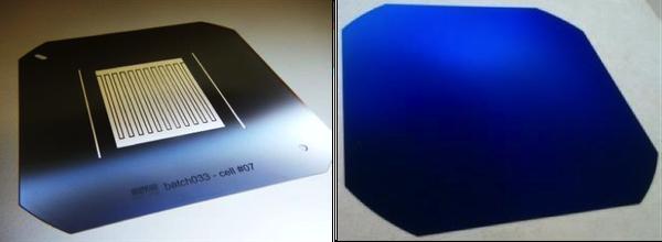
In the quest for more efficient crystalline silicon solar cells with low manufacturing costs, one of the most promising approach is to bring all electrical contacts at the back of the device. This suppresses all shadowing at the front, increasing the current and the efficiency. This approach generally requires several delicate processing steps, because well-defined narrow negative and positive contact lines need to be created, which will then collect the electrons (negative charges) and holes (positive charges). This requires usually several steps of masking of photolithography to create the alternated positive (+) and negative (-) areas.
The team at the EPFL Photovoltaics laboratory and at the CSEM PV-center succeeded in establishing an innovative process in which the positive and negative contacts align automatically. This is made possible by depositing the first “negative” contact by plasma process through a mask. Subsequently, a second layer (positive) is deposited over the full surface. The growth of this layer is such that the negative contact, even covered with the positive contact, remains negative.
Using this simple process, 25-cm2 solar cells have already reached 23.2% efficiency, with the potential of reaching almost 26%. The researchers work with the Meyer Burger Company, a leading manufacturer of equipment for solar cell production lines, to work out industrial solutions for such solar cells, valorizing the so-called silicon heterojunctions technology that serve as the basis of this work.
The research was funded by the Meyer Burger Company, the Commission for Technology and Innovation (CTI) and the Swiss Federal Office of Energy (SFOE). The work will continue as part of the European project H2020 Nextbase.
-----
Reference
"Simple processing of back-contacted silicon heterojunction solar cells using selective-area crystalline growth". Andrea Tomasi, Bertrand Paviet-Salomon, Quentin Jeangros, Jan Haschke, Gabriel Christmann, Loris Barraud, Antoine Descoeudres, Johannes Peter Seif, Sylvain Nicolay, Matthieu Despeisse, Stefaan De Wolf & Christophe Ballif
Nature Energy 2, Article number: 17062 (2017)

Back of the solar cell, with positive and negative electrical contact.
Front of the cell with no shadowing.