
A New Organic Spacer for Layered Perovskite Solar Cells
© 2026 EPFL
LIMNO researchers have designed a visible-light-absorbing organic spacer that turns the layered “2D” perovskites into an active part of the solar cell, extending light harvesting to 650 nm and boosting performance five-fold over conventional spacers.
Researchers at the Laboratory for Molecular Engineering of Optoelectronic Nanomaterials (LIMNO) at EPFL, together with collaborators at the University of Bern, have designed a new organic spacer molecule that turns a normally spectroscopic silent components of layered perovskite solar cells into a light-harvesting active material.
Layered perovskites, often called "2D perovskites", consist of alternating organic and inorganic layers. Typically, the organic molecules do not absorb sunlight and they hinder the charge transport between the inorganic slabs of the layered perovskite.
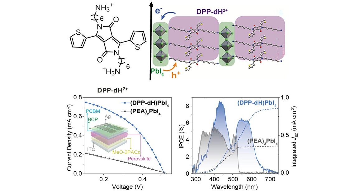
In this work, published in Advanced Materials, the team led by Waygen Thor and Colin Jeanguenat designed a spacer cation based on a diketopyrrolopyrrole (DPP) core, a well-known organic semiconductor for its strong absorption deep into the visible range. By carefully tuning the length of the alkyl chain linking the DPP core, the researchers identified a dihexyl-substituted length as the right size to be incorporated into an ordered layered perovskite structure (DPP-dH)PbI4.
The resulting material absorbs light through both its organic and inorganic components, exhibiting a type-II heterojunction bidirectional charge transfer: exciting the perovskite slab transfers holes into the organic layer, while exciting the organic spacer transfers electrons into the inorganic slabs. This bidirectional charge transfer produces long-lived free carriers and reduces trap density compared to conventional spacers, besides pushing the solar cell light response beyond the reach of conventional layered perovskites to 650 nm. Devices built with the new spacer achieved a five-fold improvement in power conversion efficiency over those made with the conventional phenethylammonium (PEA) spacer, alongside better resistance to heat and humidity.
This work establishes visible-light-absorbing, semiconducting spacers as a design strategy for layered perovskites, offering a path toward more efficient and durable next-generation optoelectronic devices.