A multilayer cantilever for nanoscale sensing

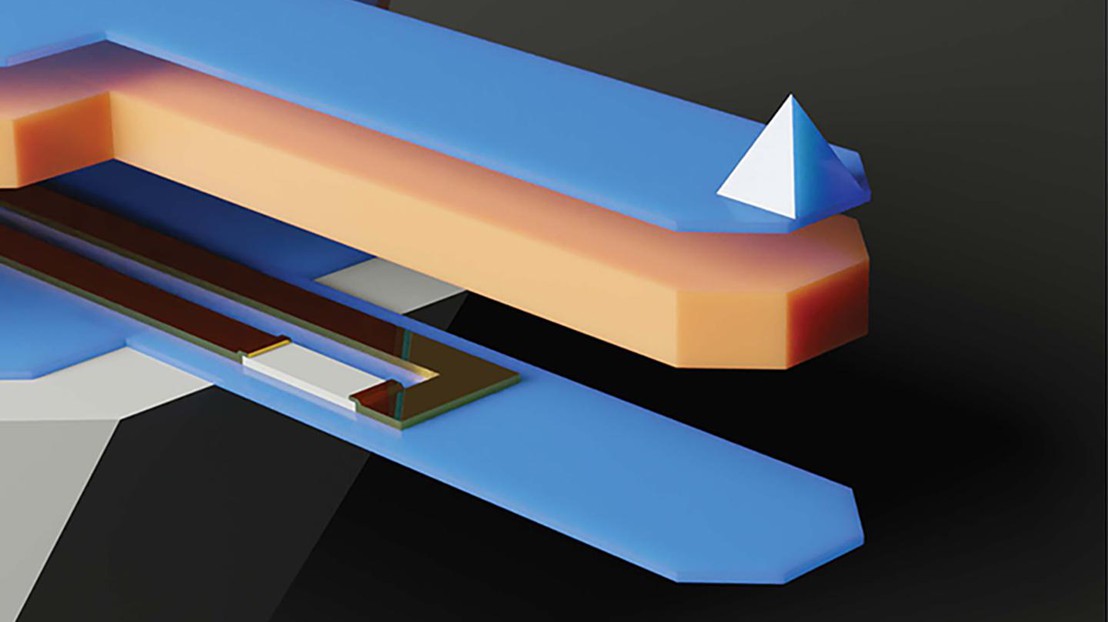
The LBNI's multilayer self-sensing cantilever © LBNI EPFL
An innovative layered concept for nanoscale sensing devices, developed by an EPFL postdoc, promises to bring greater speed, sensitivity, and functionality to applications ranging from semiconductor manufacturing to medical diagnostics.
Cantilevers are essential components of micromechanical systems, or MEMS: tiny, yet powerful devices that integrate both electronic and mechanical parts. Shaped like a beam with one fixed end, a cantilever’s free end serves as a probe to interact with a sample surface.
In atomic force microscopy, for example, the force between a cantilever and a sample can be measured using a laser beam reflected off the back of the cantilever, or using a self-sensing cantilever. However, despite the advantage of eliminating the need for a laser setup, self-sensing cantilevers have not been widely adopted due to their limited sensitivity and functionality.
Now, postdoctoral researcher Nahid Hosseini and the Laboratory for Bio- and Nano-Instrumentation (LBNI), led by Georg Fantner in EPFL’s School of Engineering, have overcome this challenge. They have pioneered a microfabrication process to create multilayer self-sensing cantilevers featuring a polymer core sandwiched between two ceramic layers. The on-chip strain sensors are integrated and sealed within the cantilever structure, enhancing both robustness and functionality.
“In addition to a sixfold reduction in force noise and improved deflection sensitivity compared to traditional silicon self-sensing cantilevers, our design protects the sensing electronics between the polymer core and the ceramic layer, meaning it can be used for imaging even in liquid environments that are chemically harsh, opaque, or electrically conductive," Hosseini says.
The teams’ innovative microfabrication platform has been published in Nature Electronics.
Rapid analysis for quality control or cancer screening
To test their device, the researchers imaged the compound eye of a wasp, and compared the results with those from a conventional cantilever. Not only did the multilayer self-sensing cantilever detect the sample topography with great accuracy, yielding significantly higher-quality images, but it did so 16 times faster than the conventional cantilever.

“The soft polymer core makes our multilayer cantilever both faster and more sensitive, because it can be made thicker without becoming stiff. Oscillations dampen, or fade more quickly with a thicker cantilever, enabling much faster surface analysis,” Hosseini explains.
Prototypes of the multilayer cantilever have already sparked the interest of international companies, and Hosseini has been fabricating the devices for various sectors. Now that the design is patented, she hopes to launch a spin-off within the next year to start building on its potential. Immediate applications include in the semiconductor industry, for example for in-line quality control, and in diagnostic medicine: the self-sensing cantilever’s unique fluid-compatibility means it could be a game-changer for rapid blood or tissue analysis.
“Developing this technology during my PhD, while also welcoming and raising my two children, has been a journey fueled by both my professional and personal support networks,” Hosseini reflects. “Our self-sensing cantilever offers unparalleled capabilities that aren't available in any current commercial devices. Now, my goal is to make this technology accessible to a broader range of users.”
Hosseini, N., Neuenschwander, M., Adams, J.D. et al. A polymer–semiconductor–ceramic cantilever for high-sensitivity fluid-compatible microelectromechanical systems. Nat Electron (2024). https://doi.org/10.1038/s41928-024-01195-z