Modelling periodic nanostructures

© 2014 EPFL
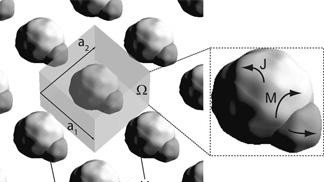
A surface integral formulation for light scattering on periodic structures is presented. Electric and magnetic field equations are derived on the scatterers’ surfaces in the unit cell with periodic boundary conditions. The solution is calculated with the method of moments and relies on the evaluation of the periodic Green’s function performed with Ewald’s method. The accuracy of this approach is assessed in detail. With this versatile boundary element formulation, a very large variety of geometries can be simulated, including doubly periodic structures on substrates and in multilayered media. The surface discretization shows a high flexibility, allowing the investigation of irregular shapes including fabrication accuracy. Deep insights into the extreme near-field of the scatterers as well as in the corresponding far-field are revealed. This method will find numerous applications for the design of realistic photonic nanostructures, in which light propagation is tailored to produce novel optical effects.
Over the year, the NAM has devoted a lot of efforts to the development of original and robust computational techniques to study the interaction of light with complex nanostructures. Our most recent contribution is a technique able to handle periodic structures with a periodicity in 1, 2 and 3 dimensions.
This approach is based on a surface integral formulation. Electric and magnetic field equations are derived on the scatterers’ surfaces in the unit cell with periodic boundary conditions. The solution is calculated with the method of moments and relies on the evaluation of the periodic Green’s function performed with Ewald’s method. The accuracy of this approach is assessed in detail. With this versatile boundary element formulation, a very large variety of geometries can be simulated, including doubly periodic structures on substrates and in multilayered media. The surface discretization shows a high flexibility, allowing the investigation of irregular shapes including fabrication accuracy. Deep insights into the extreme near-field of the scatterers as well as in the corresponding far-field are revealed. This method will find numerous applications for the design of realistic photonic nanostructures, in which light propagation is tailored to produce novel optical effects.

The previous figure shows a typical example where light is scattered scattered by a photonic crystal made with an infinite square array of pillars with a refractive index of 3.36 in air. The real part of the total (incident+scattered) instantaneous electric field is calculated in planes at 500 nm above, 500 nm below, and in the array for a 45° p-polarized plane wave incident from above. The scale is normalized in each frame. The arrow length is proportional to the electric field. (a),(b) No substrate; (c),(d) with substrate. Different illumination wavelengths λ are considered: (a) λ=350 nm, (b) λ=700 nm, (c) λ=340 nm, (d) λ=700 nm.
 This approach is extremely versatile and can handle almost any type of periodic geometry, with a reasonable computational cost, since only the scatterers'surfaces must be discretized. This way it is possible to handle infinite surfaces or to investigate subtle effects such as negative refraction. This is illustrated in the figure on the left, a fishnet metamaterial (unit cell discretized with 1352 triangular meshes) with a period a=300 nm incorporating two Ag layers (thickness t=40 nm) separated with a MgF2 layer (thickness s=17 nm). The right part of the figure shows the effective refractive index of this metamaterial as a function of the wavelength. This metamaterial exhibits a negative refractive index for wavelengths between 786 and 796nm. The index reaches -0.3 at λ=790nm, for a figure of merit of 0.4.
With this versatile formulation, a very large variety of geometries can be simulated, including doubly periodic structures on substrates and in multilayered media. The surface discretization provides a high flexibility, allowing the investigation of irregular shapes, including fabrication accuracy. Another advantage of the formulation is that it can give insight into the extreme near-field of the scatterers, while providing at the same time the corresponding far-field. This method shall find numerous applications for the design of realistic photonic and plasmonic nanostructures, in which light propagation is tailored to produce novel optical effects.
Check the corresponding publication: PDF External link: doi: 10.1364/JOSAA.27.002261