Crystalline highways for photoelectrons in solar panels

© 2016 EPFL
EPFL researchers develop a method that can automate the production of perovskite nanowire chips – ideal for solar panels, lasers and a host of other technologies.
Nanowires are extremely thin wires (10-9 meters-thick) but with variable length. They are used in sensors, nanoelectronics, photonics, and renewable energy. In general, nanowires are superior in performance as compared to polycrystalline materials, which are used in similar applications. However, manufacturing nanowires can be difficult to standardize. EPFL scientists have now developed a standardized method for controlling the growth of nanowires from perovskites, which are extremely promising materials in solar-cell technology. The method, which can be automated on an industrial scale to fabricate chips, is published in the Nature journal Scientific Reports.
Researchers at László Forró’s lab at EPFL, led by postdoc Endre Horváth, guided the growth of perovskite nanowires with nanofluidic channels. These are part of a tiny, chip-mounted circuitry allowing the control and manipulation of fluids on a nanometer scale.
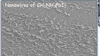
The researchers were building on their previous work, when in 2014 they used a single-step, “slip-coating” method to produce the first ever nanowires from methylammonium lead iodide. This material has attracted overwhelming attention for its ability to absorb light and produce electrical current in response.
Nanowires are so thin that they can be considered as one-dimensional structures, perovskite nanowires make outstanding candidates for the efficient transport of electrons and excitons – the recyclable “holes” that electrons leave behind when they move as a current. “A major advantage of nanowires over nanoparticles is that the evacuation of photoinduced carriers towards the electrodes is much more efficient,” says Massimo Spina, who fabricated the nanofluidic channels. “Nanowires serve as direct conductive highways, and the charges have a much higher probability to arrive at the electrodes and create an electric current.”
The fundamental problem is that it is difficult to grow the billions of nanowires needed for applications with the exact same length and diameter. “We need nanowires that resembling each other as identical twins,” says Endre Horváth. “And even we could do this, it would still leave us with the problem of growing and organizing billions of identical nanowires on a surface with extremely high precision.” The challenge therefore is to control the growth of perovskite nanowires in a way that can produce a two-dimensional actual surface that could be used in a solar cell.
Using nanofluidic channels in an automated way, the researchers were able to produce tens of thousands of parallel nanowires on a silicon surface. The growth process was visualized in real-time with a simple optical microscope, which shed light into the crystal growth mechanism.
The technique represents a great leap forward in nanowire technology. Because it is automated, it also paves the way towards fabrication of wafer-scale perovskite nanowire thin films, which are ideal for solar cells, but also for other optoelectronic devices, including lasers, light-emitting diodes (LEDs) and light detectors.
This work was funded by the Swiss National Science Foundation and the European Research Council (PICOPROP). Device fabrication was carried out in part at EPFL’s Center for Micro/Nanotechnology (CMI).
Reference
Spina M, Bonvin E, Sienkiewicz A, Forró L, Horváth E. Controlled growth of CH3NH3PbI3 nanowires in arrays of open nanofluidic channels.Scientific Reports 6:19834 25 January 2016. DOI: 10.1038/srep19834