Bending plasmons around the corner

© 2014 EPFL
Using a finite-element, full-wave modeling approach, we present a flexible method of analyzing and simulating dielectric and plasmonic waveguide structures as well as their mode coupling. This method is applied to an integrated plasmonic circuit where a straight dielectric waveguide couples through a straight hybrid long-range plasmon waveguide to a uniformly bent hybrid one. The hybrid waveguide comprises a thin metal core embedded in a two–dimensional dielectric waveguide. The performance of such plasmonic circuits in terms of insertion losses is discussed.
The transmission and processing of information in the form of surface plasmon-polaritons on metallic waveguides holds great promises. For integration, such metallic waveguides can be easily integrated in conventional CMOS technology or combined with plastic electronics. In the framework of a collaboration with Duke University, we have investigated the integration of plasmonic waveguides in polymer technology. Using a finite-element, full-wave modeling approach, we have analyzied dielectric and plasmonic waveguide structures as well as their mode coupling. The key module for a functional plasmonic circuit, including a straight dielectric waveguide coupled through a straight hybrid long-range plasmon waveguide to a uniformly bent hybrid plasmonic mode, is simulated in detail and the performance of such plasmonic circuits in terms of insertion losses is discussed.

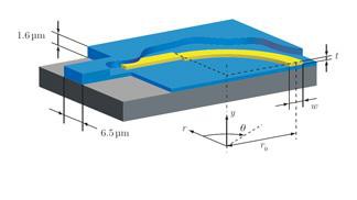
This figure shows on the left the structure investigated, comprising an conventional integrated photonic waveguide coupled into a straight and then a bent hybrid plasmonic waveguide in polymer technology. On the right, the coupling efficiency between the photonic and plasmonic waveguides depends on the position of the plasmonic strip with respect to the optical waveguide.
Check the corresponding publication: PDF External link: doi: 10.1364/OE.19.018979