A breakthrough in plasmonics

© 2013 EPFL
EPFL scientists have discovered how optical signal transmission can be controlled, paving the way for the integration of plasmonics with conventional electronic circuits.
When light hits a metal under certain circumstances, it generates a density wave of the electrons on its surface, like throwing a stone in water. This wave is called a plasmon, and it is small and rapid, occurring at optical frequencies. Plasmonics, the study of plasmons, has gained tremendous interest worldwide as it might offer a way to bridge electronic and optical circuits in technologies like computers, creating superfast processors. However, integrating plasmonics with regular electronic circuits requires the ability to control the plasmons. In an exciting Nano Letters publication, EPFL scientists collaborating with the Max Plank Institute have found how plasmons can be controlled in terms of energy and space.
Optical fibers have already changed the way we communicate by using light to transmit digital data and high bandwidths and across long distances, but require relatively bulky “wires” that are essentially four-layer tubes with reflective interiors. On the other hand, electrical wires are thinner and easier to manufacture, but transmit data at a much lower rate. Plasmonics hold the potential to bridge optics with electronics and combine their benefits without their disadvantages.
The idea is simple: use light to encode and transmit data at optical frequencies across the surface of a conventional electrical wire. Often referred to as “light on a wire”, plasmonics has become a rapidly growing field that promises many exciting new technologies. These include extremely sensitive biosensors, significantly improved telecommunications and a new generation of computer processors that can operate at ultrafast speeds. Since plasmons are waves of excited surface electrons rather than movement of actual particles, plasmonic transmission can be orders of magnitude faster than electronic transmission.
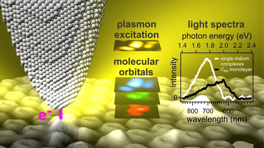
Scientists from the Max-Planck-EPFL Center for Molecular Nanoscience and Technology have now brought us a step closer to an era of plasmonics by showing that the molecular orbitals of a metal’s surface act as tiny gates that can control plasmons energetically and spatially. The greatest obstacle in integrating plasmonics into conventional electronic circuits is that prototype devices have to be nanoconstructed. This means that they require controllable interfaces between nanoelectronics and nano-optics. The researchers found that the solution lies in the individual molecular orbitals: mathematical functions that describe the electron clouds that form when atoms join together in a molecule.
Led by Klaus Kern, the team used a scanning tunneling microscope (STM) to examine iridium complexes cooled down to an absolute zero temperature (5 degrees Kelvin). STM microscopy exploits the tunneling of electrons from a metal surface to a very sharp metallic tip that can be scanned over the metal’s surface. On their way to the tip, some of the electrons lose energy. This energy excites oscillations (plasmons) at the metal surface and the tip and can be then observed by the emission of light into an optical detector.
The team’s data showed that the excitation of plasmons can be actively controlled by a single molecule. Studying an iridium complex, they discovered that its molecular orbitals – effectively the particular energy levels – act as tiny gates that determine the generation of plasmons both energetically and spatially, even down to areas smaller than the molecule itself. In fact, in molecules whose electron structure is known, both the energy and the location of generated oscillations can be predicted, meaning that it is now possible to actually control the generation of plasmons on the single-molecule level.
The scientists believe that this phenomenon is not restricted solely to the iridium complex, but should also apply to other organic molecules. The discovery will have a significant impact on the design of future plasmon-based devices, as it paves the way to control the electrical excitation of plasmonic nanostructures down to, and even below, the level of an individual molecule, and can allow the direct integration of plasmonic nanostructures into conventional electronic circuits.